 Your new post is loading...
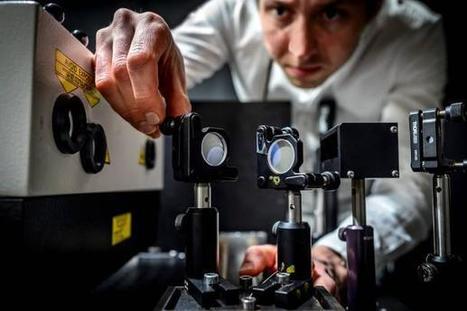
A new technique greatly reduces the error in an optical neural network, which uses light to process data instead of electrical signals. With their technique, the larger an optical neural network becomes, the lower the error in its computations. This could enable them to scale these devices up so they would be large enough for commercial uses. As machine-learning models become larger and more complex, they require faster and more energy-efficient hardware to perform computations. Conventional digital computers are struggling to keep up. An analog optical neural network could perform the same tasks as a digital one, such as image classification or speech recognition, but because computations are performed using light instead of electrical signals, optical neural networks can run many times faster while consuming less energy. However, these analog devices are prone to hardware errors that can make computations less precise. Microscopic imperfections in hardware components are one cause of these errors. In an optical neural network that has many connected components, errors can quickly accumulate. Even with error-correction techniques, due to fundamental properties of the devices that make up an optical neural network, some amount of error is unavoidable. A network that is large enough to be implemented in the real world would be far too imprecise to be effective. MIT researchers have overcome this hurdle and found a way to effectively scale an optical neural network. By adding a tiny hardware component to the optical switches that form the network’s architecture, they can reduce even the uncorrectable errors that would otherwise accumulate in the device. Their work could enable a super-fast, energy-efficient, analog neural network that can function with the same accuracy as a digital one. With this technique, as an optical circuit becomes larger, the amount of error in its computations actually decreases. “This is remarkable, as it runs counter to the intuition of analog systems, where larger circuits are supposed to have higher errors, so that errors set a limit on scalability. This present paper allows us to address the scalability question of these systems with an unambiguous ‘yes,’” says lead author Ryan Hamerly, a visiting scientist in the MIT Research Laboratory for Electronics (RLE) and Quantum Photonics Laboratory and senior scientist at NTT Research. Hamerly’s co-authors are graduate student Saumil Bandyopadhyay and senior author Dirk Englund, an associate professor in the MIT Department of Electrical Engineering and Computer Science (EECS), leader of the Quantum Photonics Laboratory, and member of the RLE. The research is published today in Nature Communications.
A new method of building materials using light, developed by researchers at the University of Cambridge, could one day enable technologies that are often considered the realm of science fiction, such as invisibility cloaks and cloaking devices.
Although cloaked starships won't be a reality for quite some time, the technique which researchers have developed for constructing materials with building blocks a few billionths of a meter across can be used to control the way that light flies through them, and works on large chunks all at once. Details are published today (28 July, 2015) in the journal Nature Communications.
The key to any sort of 'invisibility' effect lies in the way light interacts with a material. When light hits a surface, it is either absorbed or reflected, which is what enables us to see objects. However, by engineering materials at the nanoscale, it is possible to produce 'metamaterials': materials which can control the way in which light interacts with them. Light reflected by a metamaterial is refracted in the 'wrong' way, potentially rendering objects invisible, or making them appear as something else.
Metamaterials have a wide range of potential applications, including sensing and improving military stealth technology. However, before cloaking devices can become reality on a larger scale, researchers must determine how to make the right materials at the nanoscale, and using light is now shown to be an enormous help in such nano-construction.
The technique developed by the Cambridge team involves using unfocused laser light as billions of needles, stitching gold nanoparticles together into long strings, directly in water for the first time. These strings can then be stacked into layers one on top of the other, similar to Lego bricks. The method makes it possible to produce materials in much higher quantities than can be made through current techniques.
In order to make the strings, the researchers first used barrel-shaped molecules called cucurbiturils (CBs). The CBs act like miniature spacers, enabling a very high degree of control over the spacing between the nanoparticles, locking them in place.
In order to connect them electrically, the researchers needed to build a bridge between the nanoparticles. Conventional welding techniques would not be effective, as they cause the particles to melt. "It's about finding a way to control that bridge between the nanoparticles," said Dr Ventsislav Valev of the University's Cavendish Laboratory, one of the authors of the paper. "Joining a few nanoparticles together is fine, but scaling that up is challenging."
The key to controlling the bridges lies in the cucurbiturils: the precise spacing between the nanoparticles allows much more control over the process. When the laser is focused on the strings of particles in their CB scaffolds, it produces plasmons: ripples of electrons at the surfaces of conducting metals. These skipping electrons concentrate the light energy on atoms at the surface and join them to form bridges between the nanoparticles. Using ultrafast lasers results in billions of these bridges forming in rapid succession, threading the nanoparticles into long strings, which can be monitored in real time.
"We have controlled the dimensions in a way that hasn't been possible before," said Dr Valev, who worked with researchers from the Department of Chemistry and the Department of Materials Science & Metallurgy on the project. "This level of control opens up a wide range of potential practical applications."
Via Anne Pascucci, MPA, CRA, Mark E. Deschaine, PhD, Jocelyn Stoller
Hologram technology already exists. Whatever is not yet sufficiently advanced, however, we have witnessed some progress in this area as: hologram created in mid air by laser, 3D hologram displays, holograms in the toy industry and the like. Unfortunately Hologram display can not be touched and interaction with it would feel more natural.
That at least was true till now when a Japanese team of scientists from Digital Nature Group managed to create a hologram display that you can touch. The concept is similar to the hologram which was created in mid air (also in Japan). Namely, the laser is used to create display emits superfast and supershort radiation (measured in femtoseconds). These radiations wiggle molecules of air, while helping to ionize (resulting in their lighting). As we know, a set of ionized particles to a place called plasma, which is generated by the laser.
The very fact that the molecules are forced to move in the air is causing the ability to touch them. Namely, when you put a finger in the hologram air, molecules are hitting your skin and you feel like it you touched something. According to lead author of the study it feels like you're touching sand paper or electrostatic shock. Additionally, by using a camera which is placed under the display you can recognize when you touched the display and where, and to convey the command somewhere in the software.
Scientists say that they have chosen femtosecond display nanoseconds because it is safer for the skin because there is not enough time to warm up and damage. This will allow interactive 3D holograms that can be touched, which will contribute to significant progress in hologram technology. The projection of such holograms may allow upgrading of our reality in the case if these kind of devices are placed all around us and project images and objects that we could touch.
This femtosecond laser-based volumetric display will be demonstrated to the public as a part of the Siggraph 2015 exhibition in August.
Researchers at Eindhoven University of Technology (TU/e) in the Netherlands and the University of Central Florida (CREOL), report in the journal Nature Photonics the successful transmission of a record high 255 Terabits/s over a new type of fiber allowing 21 times more bandwidth than currently available in communication networks. This new type of fiber could be an answer to mitigating the impending optical transmission capacity crunch caused by the increasing bandwidth demand.
Due to the popularity of Internet services and emerging network of capacity-hungry datacentres, demand for telecommunication bandwidth is expected to continue at an exponential rate. To transmit more information through current optical glass fibers, an option is to increase the power of the signals to overcome the losses inherent in the glass from which the fibre is manufactured. However, this produces unwanted photonic nonlinear effects, which limit the amount of information that can be recovered after transmission over the standard fiber.
The team at TU/e and CREOL, led by dr. Chigo Okonkwo, an assistant professor in the Electro-Optical Communications (ECO) research group at TU/e and dr. Rodrigo Amezcua Correa, a research assistant professor in Micro-structured fibers at CREOL, demonstrate the potential of a new class of fiber to increase transmission capacity and mitigate the impending 'capacity crunch' in their article that appeared yesterday in the online edition of the journal Nature Photonics.
The new fiber has seven different cores through which the light can travel, instead of one in current state-of-the-art fibers. This compares to going from a one-way road to a seven-lane highway. Also, they introduce two additional orthogonal dimensions for data transportation – as if three cars can drive on top of each other in the same lane. Combining those two methods, they achieve a gross transmission throughput of 255 Terabits/s over the fiber link. This is more than 20 times the current standard of 4-8 Terabits/s.
A pair of breakthroughs in the field of silicon photonics by researchers at the University of Colorado Boulder, the Massachusetts Institute of Technology and Micron Technology Inc. could allow for the trajectory of exponential improvement in microprocessors that began nearly half a century ago—known as Moore's Law—to continue well into the future, allowing for increasingly faster electronics, from supercomputers to laptops to smartphones.
The research team, led by CU-Boulder researcher Milos Popovic, an assistant professor of electrical, computer and energy engineering, developed a new technique that allows microprocessors to use light, instead of electrical wires, to communicate with transistors on a single chip, a system that could lead to extremely energy-efficient computing and a continued skyrocketing of computing speed into the future. Popovic and his colleagues created two different optical modulators—structures that detect electrical signals and translate them into optical waves—that can be fabricated within the same processes already used in industry to create today's state-of-the-art electronic microprocessors. The modulators are described in a recent issue of the journal Optics Letters. First laid out in 1965, Moore's Law predicted that the size of the transistors used in microprocessors could be shrunk by half about every two years for the same production cost, allowing twice as many transistors to be placed on the same-sized silicon chip. The net effect would be a doubling of computing speed every couple of years. The projection has held true until relatively recently. While transistors continue to get smaller, halving their size today no longer leads to a doubling of computing speed. That's because the limiting factor in microelectronics is now the power that's needed to keep the microprocessors running. The vast amount of electricity required to flip on and off tiny, densely packed transistors causes excessive heat buildup. "The transistors will keep shrinking and they'll be able to continue giving you more and more computing performance," Popovic said. "But in order to be able to actually take advantage of that you need to enable energy-efficient communication links."
|
Forget high-speed cameras capturing 100 000 images per second. A research group at Lund University in Sweden has developed a camera that can film at a rate equivalent to five trillion images per second, or events as short as 0.2 trillionths of a second. This is faster than has previously been possible. The new super-fast film camera will therefore be able to capture incredibly rapid processes in chemistry, physics, biology and biomedicine, that so far have not been caught on film. To illustrate the technology, the researchers have successfully filmed how light – a collection of photons – travels a distance corresponding to the thickness of a paper. In reality, it only takes a picosecond, but on film the process has been slowed down by a trillion times. Currently, high-speed cameras capture images one by one in a sequence. The new technology is based on an innovative algorithm, and instead captures several coded images in one picture. It then sorts them into a video sequence afterwards. In short, the method involves exposing what you are filming (for example a chemical reaction) to light in the form of laser flashes where each light pulse is given a unique code. The object reflects the light flashes which merge into the single photograph. They are subsequently separated using an encryption key. The film camera is initially intended to be used by researchers who literally want to gain better insight into many of the extremely rapid processes that occur in nature. Many take place on a picosecond and femtosecond scale, which is unbelievably fast – the number of femtoseconds in one second is significantly larger than the number of seconds in a person’s life-time. “This does not apply to all processes in nature, but quite a few, for example, explosions, plasma flashes, turbulent combustion, brain activity in animals and chemical reactions. We are now able to film such extremely short processes”, says Elias Kristensson. “In the long term, the technology can also be used by industry and others”.
A team of scientists has successfully measured particles of light being “squeezed”, in an experiment that had been written off in physics textbooks as impossible to observe.
Squeezing is a strange phenomenon of quantum physics. It creates a very specific form of light which is “low-noise” and is potentially useful in technology designed to pick up faint signals, such as the detection of gravitational waves.
The standard approach to squeezing light involves firing an intense laser beam at a material, usually a non-linear crystal, which produces the desired effect.
For more than 30 years, however, a theory has existed about another possible technique. This involves exciting a single atom with just a tiny amount of light. The theory states that the light scattered by this atom should, similarly, be squeezed.
Unfortunately, although the mathematical basis for this method – known as squeezing of resonance fluorescence – was drawn up in 1981, the experiment to observe it was so difficult that one established quantum physics textbook despairingly concludes: “It seems hopeless to measure it”.
So it has proven – until now. In the journal Nature, a team of physicists report that they have successfully demonstrated the squeezing of individual light particles, or photons, using an artificially constructed atom, known as a semiconductor quantum dot. Thanks to the enhanced optical properties of this system and the technique used to make the measurements, they were able to observe the light as it was scattered, and proved that it had indeed been squeezed.
Professor Mete Atature, from the Cavendish Laboratory, Department of Physics, and a Fellow of St John’s College at the University of Cambridge, led the research. He said: “It’s one of those cases of a fundamental question that theorists came up with, but which, after years of trying, people basically concluded it is impossible to see for real – if it’s there at all.”
“We managed to do it because we now have artificial atoms with optical properties that are superior to natural atoms. That meant we were able to reach the necessary conditions to observe this fundamental property of photons and prove that this odd phenomenon of squeezing really exists at the level of a single photon. It’s a very bizarre effect that goes completely against our senses and expectations about what photons should do.”
Most lenses are, by definition, curved. After all, they are named for their resemblance to lentils, and a glass lens made flat is just a window with no special powers. But a new type of lens created at the Harvard School of Engineering and Applied Sciences(SEAS) turns conventional optics on its head.
A major leap forward from a prototype device demonstrated in 2012, it is an ultra-thin, completely flat optical component made of a glass substrate and tiny, light-concentrating silicon antennas. Light shining on it bends instantaneously, rather than gradually, while passing through. The bending effects can be designed in advance, by an algorithm, and fine-tuned to fit almost any purpose.
With this new invention described today in Science, the Harvard research team has overcome an inherent drawback of a wafer-thin lens: light at different wavelengths (i.e., colors) responds to the surface very differently. Until now, this phenomenon has prevented planar optics from being used with broadband light. Now, instead of treating all wavelengths equally, the researchers have devised a flat lens with antennas that compensate for the wavelength differences and produce a consistent effect—for example, deflecting three beams of different colors by the same angle, or focusing those colors on a single spot.
“What this now means is that complicated effects like color correction, which in a conventional optical system would require light to pass through several thick lenses in sequence, can be achieved in one extremely thin, miniaturized device,” said principal investigator Federico Capasso, the Robert L. Wallace Professor of Applied Physics and Vinton Hayes Senior Research Fellow in Electrical Engineering at Harvard SEAS.
The realisation of quantum networks is one of the major challenges of modern physics. Now, new research shows how high-quality photons can be generated from ‘solid-state’ chips, bringing us closer to the quantum ‘Internet’. We are at the dawn of quantum-enabled technologies, and quantum computing is one of many thrilling possibilities. The number of transistors on a microprocessor continues to double every two years, amazingly holding firm to a prediction by Intel co-founder Gordon Moore almost 50 years ago. If this is to continue, conceptual and technical advances harnessing the power of quantum mechanics in microchips will need to be investigated within the next decade. Developing a distributed quantum network is one promising direction pursued by many researchers today. A variety of solid-state systems are currently being investigated as candidates for quantum bits of information, or qubits, as well as a number of approaches to quantum computing protocols, and the race is on for identifying the best combination. One such qubit, a quantum dot, is made of semiconductor nanocrystals embedded in a chip and can be controlled electro-optically. Single photons will form an integral part of distributed quantum networks as flying qubits. First, they are the natural choice for quantum communication, as they carry information quickly and reliably across long distances. Second, they can take part in quantum logic operations, provided all the photons taking part are identical. Unfortunately, the quality of photons generated from solid-state qubits, including quantum dots, can be low due to decoherence mechanisms within the materials. With each emitted photon being distinct from the others, developing a quantum photonic network faces a major roadblock. Now, researchers from the Cavendish Laboratory at Cambridge University have implemented a novel technique to generate single photons with tailored properties from solid-state devices that are identical in quality to lasers. Their research is published today in the journal Nature Communications. As their photon source, the researchers built a semiconductor Schottky diode device containing individually addressable quantum dots. The transitions of quantum dots were used to generate single photons via resonance fluorescence – a technique demonstrated previously by the same team. Under weak excitation, also known as the Heitler regime, the main contribution to photon generation is through elastic scattering. By operating in this way, photon decoherence can be avoided altogether. The researchers were able to quantify how similar these photons are to lasers in terms of coherence and waveform – it turned out they were identical. “Our research has added the concepts of coherent photon shaping and generation to the toolbox of solid-state quantum photonics,” said Dr Mete Atature from the Department of Physics, who led the research. “We are now achieving a high-rate of single photons which are identical in quality to lasers with the further advantage of coherently programmable waveform - a significant paradigm shift to the conventional single photon generation via spontaneous decay.” There are already protocols proposed for quantum computing and communication which rely on this photon generation scheme, and this work can be extended to other single photon sources as well, such as single molecules, colour centres in diamond and nanowires. “We are at the dawn of quantum-enabled technologies, and quantum computing is one of many thrilling possibilities,” added Atature.
|


Buy Metformin online
Buy mifeprex online
Mifepristone (also known as RU 486) is used to cause an abortion during the early part of pregnancy. It is used up to week 10 of pregnancy (up to 70 days after the first day of your last menstrual period).$519.00 $360.00Buy mounjaro injectable pens
Buy mtp kit pills online
the process is also termed as ending an undesired pregnancy using abortion pills. It is the safest alternative to surgical abortion. Women who do not wish to go for surgery can go for medical abortion with MTP Kit if the gestation week is within 8 weeks.$590.00 $250.00Buy Myrbetriq online
Myrbetriq is a brand-name drug of Mirabegron. This medicine is used to treat the symptoms of overactive bladder such as frequent urination or sudden need to urinate. Tell your doctor about all your medical conditions before starting Myrbetriq.$320.00 $200.00Buy naltrexone contrave
Our online pharmacy is well known among our customers for being the best one available. Naltrexone to make you can charge to know where those who drive, etc. Where those patients feel funny.$300.00 $200.00Buy Opana online
Opana ER, also available as Numorphan or Opana, is an opioid medication. It helps treat moderate to severe pain. The extended-release form of oxymorphone is for around-the-clock treatment of pain or should not use-as-needed basis for pain.$540.00 $220.00Buy Ozempic online
Ozempic is a brand name for Semaglutide which is used in the treatment of type 2 diabetes. It belongs to a class of drugs called anti-diabetics, Glucagon-like Peptide-1 Agonists.$439.99 $320.99Buy Percocet Pills Online
$500.00 $300.00Buy Plavix Online
$470.99 $240.99Buy Plavix or Generic Online
$400.00 $210.00Buy pure gbl gamma-butyrolactone
INGREDIENTS:– CAS: 96-48-0 – EINECS: 202-509-5 – Gamma-Butyrolactone 99,9% GBL Cleaner 1000mLPRECAUTIONS FOR USE– Do not swallow. – Avoid any contact with the eyes. – Keep out of reach of children. – In case of contact with eyes, rinse immediately with clean water and consult your doctor. – Wear suitable protective clothing. – In case of accident or if you feel unwell, seek medical advice immediately.$200.00 $150.00Buy Saxenda online
$740.99 $480.99Buy Singulair online
$450.00 $214.00Buy Sustanon online
$569.00 $350.00Buy testosterone cypionate online
testosterone cypionate This medication is used in men who do not make enough of a natural substance called testosterone. In males, testosterone is responsible for many normal functions, including growth and development of the genitals, muscles, and bones. It also helps cause normal sexual development (puberty) in boys.$65.00 – $70.00