Your new post is loading...
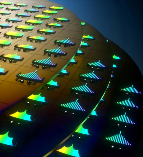
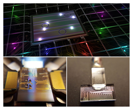
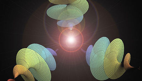
Fifteen years ago, UC Santa Barbara electrical and materials professor John Bowers pioneered a method for integrating a laser onto a silicon wafer. The technology has since been widely deployed in combination with other silicon photonics devices to replace the copper-wire interconnects that formerly linked servers at data centers, dramatically increasing energy efficiency -- an important endeavor at a time when data traffic is growing by roughly 25% per year. For several years, the Bowers group has collaborated with the group of Tobias J. Kippenberg at the Swiss Federal Institute of Technology (EPFL), within the Defense Advanced Research Projects Agency (DARPA) Direct On-Chip Digital Optical Synthesizer (DODOS) program. The Kippenberg group discovered "microcombs," a series of parallel, low-noise, highly stable laser lines. Each of the many lines of the laser comb can carry information, extensively multiplying the amount of data that can be sent by a single laser. Recently, several teams demonstrated very compact combs by placing a semiconductor laser chip and a separate silicon nitride ring-resonator chip very close together. However, the laser and the resonator were still separate devices, made independently and then placed in close proximity to each other perfectly aligned, a costly and time-consuming process that is not scalable. The Bowers lab has worked with the Kippenberg lab to develop an integrated on-chip semiconductor laser and resonator capable of producing a laser microcomb. A paper titled "Laser soliton microcombs heterogeneously integrated on silicon," published in the new issue of the journal Science, describes the labs' success in becoming the first to achieve that goal. Soliton microcombs are optical frequency combs that emit mutually coherent laser lines -- that is, lines that are in constant, unchanging phase relative to each other. The technology is applied in the areas of optical timing, metrology and sensing. Recent field demonstrations include multi-terabit-per-second optical communications, ultrafast light detection and ranging (LiDAR), neuromorphic computing, and astrophysical spectrometer calibration for planet searching, to name several. It is a powerful tool that normally requires exceptionally high power and expensive lasers and sophisticated optical coupling to function. The working principle of a laser microcomb, explained lead author Chao Xiang, a postdoctoral researcher and newly minted Ph.D. in Bowers's lab, is that a distributed feedback (DFB) laser produces one laser line. That line then passes through an optical phase controller and enters the micro-ring resonator, causing the power intensity to increase as the light travels around the ring. If the intensity reaches a certain threshold, non-linear optical effects occur, causing the one laser line to create two additional, identical lines on either side. Each of those two "side lines" creates others, leading to a cascade of laser-line generation. "You end up with a series of mutually coherent frequency combs," Xiang said -- and a vastly expanded ability to transmit data. This research enables semiconductor lasers to be seamlessly integrated with low-loss nonlinear optical micro-resonators -- "low-loss" because the light can travel in the waveguide without losing a significant amount of its intensity over distance. No optical coupling is required, and the device is entirely electrically controlled. Importantly, the new technology lends itself to commercial-scale production, because thousands of devices can be made from a single wafer using industry standard complementary metal oxide semiconductor (CMOS)-compatible techniques. "Our approach paves the way for large-volume, low-cost manufacturing of chip-based frequency combs for next-generation high-capacity transceivers, data centers, space and mobile platforms," the researchers stated.
Quantum technologies such as quantum computers require sources of entangled pairs of photons. To make these photon pairs, researchers commonly use silicon-based devices, where the silicon sits on an insulator. Galan Moody and his colleagues at the University of California, Santa Barbara, wondered if they could switch the silicon with aluminum gallium arsenide (AlGaAs), a material that has recently been demonstrated to be useful for classical photonics applications. The team showed that AlGaAs-made devices can produce entangled photons at a rate 1000 times greater than devices made from other materials [1]. Chip-sized devices for producing entangled pairs of photons typically couple laser light into a photonic waveguide or an optical cavity. Individual photons in the laser are then annihilated by interacting with the cavity’s material, a process that creates two new—entangled—photons. The efficiency of this process depends on the size of the cavity and the properties of the material used to make it. Using this same design, Moody and his colleagues tinkered with the cavity’s size and switched its material from silicon to AlGaAs. They found that they could increase the efficiency of the process significantly without compromising other important properties of the generated entangled photon pairs, such as entanglement fidelity. The 1000-fold increase in brightness that the team achieved should, they say, let them produce the same number of entangled photon pairs as other devices but by using lower-power lasers. That could allow the modified devices to consume less power overall. AlGaAs could also be used to make the other components for quantum computers, potentially allowing them to be contained on a single chip. The team says that such integration would simplify device fabrication and facilitate all-on-chip quantum-photonics systems.
Researchers from the Harvard John A. Paulson School of Engineering and Applied Sciences (SEAS), in collaboration with researchers at McMaster University and University of Pittsburgh, have developed a new platform for all-optical computing, meaning computations done solely with beams of light. "Most computation right now uses hard materials such as metal wires, semiconductors and photodiodes to couple electronics to light," said Amos Meeks, a graduate student at SEAS and co-first author of the research. "The idea behind all-optical computing is to remove those rigid components and control light with light. Imagine, for example, an entirely soft, circuitry-free robot driven by light from the sun." These platforms rely on so-called non-linear materials that change their refractive index in response to the intensity of light. When light is shone through these materials, the refractive index in the path of the beam increases, generating its own, light-made waveguide. Currently, most non-linear materials require high-powered lasers or are permanently changed by the transmission of light. Now, researchers developed a fundamentally new material that uses reversible swelling and contracting in a hydrogel under low laser power to change the refractive index. The hydrogel is composed of a polymer network that is swollen with water, like a sponge, and a small number of light-responsive molecules known as spiropyran (which is similar to the molecule used to tint transition lenses). When light is shone through the gel, the area under the light contracts a small amount, concentrating the polymer and changing the refractive index. When the light is turned off, the gel returns to its original state. When multiple beams are shone through the material, they interact and affect each other, even at large distances. Beam A could inhibit Beam B, Beam B could inhibit Beam A, both could cancel each other out or both could go through -- creating an optical logic gate. "Though they are separated, the beams still see each other and change as a result," said Kalaichelvi Saravanamuttu, an associate professor of Chemistry and Chemical Biology at McMaster and co-senior author of the study. "We can imagine, in the long term, designing computing operations using this intelligent responsiveness." "Not only can we design photoresponsive materials that reversibly switch their optical, chemical and physical properties in the presence of light, but we can use those changes to create channels of light, or self-trapped beams, that can guide and manipulate light," said co-author Derek Morim, a graduate student in Saravanamuttu's lab. "Materials science is changing," said Joanna Aizenberg, the Amy Smith Berylson Professor of Materials Science at SEAS and co-senior author of the study. "Self-regulated, adaptive materials capable of optimizing their own properties in response to environment replace static, energy-inefficient, externally regulated analogs. Our reversibly responsive material that controls light at exceptionally small intensities is yet another demonstration of this promising technological revolution."
The terahertz frequency range — which sits in the middle of the electromagnetic spectrum between microwaves and infrared light — offers the potential for high-bandwidth communications, ultrahigh-resolution imaging, precise long-range sensing for radio astronomy, and much more. But this section of the electromagnetic spectrum has remained out of reach for most applications. That is because current sources of terahertz frequencies are bulky, inefficient, have limited tuning or have to operate at low temperature. Now, researchers from the Harvard John A. Paulson School of Engineering and Applied Sciences (SEAS), in collaboration with MIT and the U.S. Army, have developed a compact, room temperature, widely tunable terahertz laser. The research was published today (November 15, 2019) in the journal Science. “This laser outperforms any existing laser source in this spectral region and opens it up, for the first time, to a broad range of applications in science and technology,” said Federico Capasso, the Robert L. Wallace Professor of Applied Physics and Vinton Hayes Senior Research Fellow in Electrical Engineering at SEAS and co-senior author of the paper. “There are many needs for a source like this laser, things like short range, high bandwidth wireless communications, very high-resolution radar, and spectroscopy,” said Henry Everitt, Senior Technologist with the U.S. Army CCDC Aviation & Missile Center and co-senior author of the paper.
A camera system that captures a snapshot of overlapping light waves in a tiny fraction of a second could lead to new methods for imaging, allowing scientists to watch the brain’s neurons interacting or see neutrinos colliding with matter. The camera system took snapshots at a rate of 100 billion frames per second, fast enough to capture a pulse of laser light spreading out in a Mach cone, the optical equivalent of the sonic boom created by an airplane traveling faster than the speed of sound. “You can think of the laser source as the supersonic jet and everything is dragged behind. Instead of generating a sound, we’re generating a scattered wavelet,” says Jinyang Liang, a postdoctoral research associate in Lihong Wang’s Optical Imaging Lab at Washington University, in St. Louis. The researchers and their collaborators from Tsinghua University in China and the University of Illinois at Urbana-Champaign describe their work in today’s issue of Science Advances. An airplane creates a Mach cone when it passes Mach 1, the speed of sound. Because the source of the noise—the plane’s engines—is moving faster than sound itself, the sound waves get compressed and spread out in a cone shape behind the aircraft. The same thing can happen to light. To generate their optical Mach cone, the researchers made two silicone display panels, which they laced with aluminum oxide powder to scatter the light toward the cameras. They placed the panels on opposite sides of an air-filled tunnel, then threw in a chunk of dry ice to create a fog meant to scatter light. The researchers then fired a laser beam through the tunnel. Because the silicone has a higher index of refraction than the air, light striking the panels moves more slowly than the light striking the fog, so the source of the light waves is “moving faster” than the waves in the silicone are, the same as with the supersonic jet.
With leading corporations now investing in highly expensive and complex infrastructures to unleash the power of quantum technologies, INRS researchers have achieved a breakthrough in a light-weight photonic system created using on-chip devices and off-the-shelf telecommunications components. In their paper published in Nature, the team demonstrates that photons can become an accessible and powerful quantum resource when generated in the form of color-entangled quDits. The system uses a small and cost-effective photonic chip fabricated through processes similar to those used for integrated electronics. With an on-chip micro-ring resonator excited by a laser, photons are emitted in pairs that share a complex quantum state. The photons are constructed in a state featuring a number of superimposed frequency components: The photons have several colors simultaneously, and the colors of each photon in a pair are linked (entangled), regardless of their separation distance. With each frequency -- or color -- representing a dimension, the photons are generated on-chip as a high-dimensional quantum state (quDit). Thus far, quantum information science has largely focused on the exploitation of qubits, based on two-dimensional systems where two states are superimposed (for example, 0 AND 1 at the same time, in contrast to classical bits, which are 0 OR 1 at any time). Working in the frequency domain allows the superposition of many more states (for example, a high-dimensional photon can be red AND yellow AND green AND blue, although the photons used here were infrared for telecommunications compatibility), enhancing the amount of information in a single photon. To date, Professor Roberto Morandotti, who leads the INRS research team, confirms the realization of a quantum system with at least one hundred dimensions using this approach, and the technology developed is readily extendable to create two-quDit systems with more than 9,000 dimensions (corresponding to 12 qubits and beyond, comparable to the state of the art in significantly more expensive/complex platforms). The use of the frequency domain for such quantum states enables their easy transmission and manipulation in optical fibre systems. "By merging the fields of quantum optics and ultrafast optical processing, we have shown that high-dimensional manipulation of these states is indeed possible using standard telecommunications elements like modulators and frequency filters," stresses telecommunications system expert Professor José Azaña, co-supervisor of the conducted research.
The angular momentum of light plays an important role in many areas, from optical trapping to quantum information. In the usual three-dimensional setting, the angular momentum quantum numbers of the photon are integers, in units of the Planck constantħ. A group of scientists now show that, in reduced dimensions, photons can have a half-integer total angular momentum. They identify a new form of total angular momentum, carried by beams of light, comprising an unequal mixture of spin and orbital contributions. The scientists demonstrate the half-integer quantization of this total angular momentum using noise measurements. They conclude that for light, as is known for electrons, reduced dimensionality allows new forms of quantization.
New device could find use in "boson-sampling" quantum computers. A source of single photons that meets three important criteria for use in quantum-information systems has been unveiled in China by an international team of physicists. Based on a quantum dot, the device is an efficient source of photons that emerge as solo particles that are indistinguishable from each other. The researchers are now trying to use the source to create a quantum computer based on "boson sampling". Devices that emit one – and only one – photon on demand play a central role in light-based quantum-information systems. Each photon must also be emitted in the same quantum state, which makes each photon indistinguishable from all the others. This is important because the quantum state of the photon is used to carry a quantum bit (qubit) of information. Quantum dots are tiny pieces of semiconductor that show great promise as single-photon sources. When a laser pulse is fired at a quantum dot, an electron is excited between two distinct energy levels. The excited state then decays to create a single photon with a very specific energy. However, this process can involve other electron excitations that result in the emission of photons with a wide range of energies – photons that are therefore not indistinguishable. This problem can be solved by exciting the quantum dot with a pulse of light at the same energy as the emitted photon. This is called resonance fluorescence, and has been used to create devices that are very good at producing indistinguishable single photons. However, this process is inefficient, and only produces a photon about 6% of the time. Now, Chaoyang Lu, Jian-Wei Pan and colleagues at the University of Science and Technology of China have joined forces with researchers in Denmark, Germany and the UK to create a resonance-fluorescence-based source that emits a photon 66% of the time when it is prompted by a laser pulse. Of these photons, 99.1% are solo and 98.5% are in indistinguishable quantum states – with both figures of merit being suitable for applications in quantum-information systems. Lu told physicsworld.com that nearly all of the laser pulses that strike the source produce a photon, but about 34% of these photons are unable to escape the device. The device was operated at a laser-pulse frequency of 81 MHz and a pulse power of 24 nW, which is a much lower power requirement than other quantum-dot-based sources. The factor-of-ten improvement in efficiency was achieved by sandwiching a quantum dot in the centre of a "micropillar" created by stacking 40 disc-like layers (see figure). Each layer is a "distributed Bragg reflector", which is a pair of mirrors that together have a thickness of one quarter the wavelength of the emitted photons. The micropillar is about 2.5 μm in diameter and about 10 μm tall, and it allowed the team to harness the "Purcell effect", whereby the rate of fluorescence is increased significantly when the emitter is placed in a resonant cavity.
A new class of lasers developed by a team that included physics researchers at Kansas State University could help scientists measure distances to faraway targets, identify the presence of certain gases in the atmosphere and send images of the earth from space. These energy-efficient lasers also are portable, produce light at difficult-to-reach wavelengths and have the potential to scale to high-powered versions. The new lasers were invented by Brian Washburn and Kristan Corwin, both associate professors of physics at Kansas State University's College of Arts & Sciences, along with Andrew Jones, a May 2012 doctoral graduate in physics, and Rajesh Kadel, a May 2014 doctoral graduate in physics. Other contributors include three University of New Mexico physics and astronomy researchers: Wolfgang Rudolf, a Regents professor and department chair, Vasudevan Nampoothiri, a research assistant professor, and Amarin Ratanavis, a doctoral student; and John Zavada, a Virginia-based optic and photonic physicist who brought them all together. The new lasers are fiber-based and use various molecular gases to produce light. They differ from traditional glass-tube lasers, which are large and bulky, and have mirrors to reflect the light. But the novel lasers use a hollow fiber with a honeycomb structure to hold gas and to guide light. This optical fiber is filled with a molecular gas, such as hydrogen cyanide or acetylene. Another laser excites the gas and causes a molecule of the excited gas to spontaneously emit light. Other molecules in the gas quickly follow suit, which results in laser light. "By putting the gas in a hollow core, we can have really high intensities of light without having to put such high amounts of power into the laser," Corwin said. "If you had a glass tube of that size and put light in it, the light would escape through the sides. It's actually the structure that makes it work." The structure also allows for portability. In contrast to traditional lasers, which are fragile and cumbersome to move, the researchers' more durable fiber laser is about the thickness of a single strand of hair and can wrap around itself for compact storage and transportation. "The smallness is nice," Washburn said. "You can wrap up the coil like a string." The invention process began when Zavada brought Washburn and Corwin, who already had expertise putting gas into hollow fibers, together with Rudolph and Nampoothiri, who were skilled in making optically pumped gas lasers. "We thought hard about how this would all work together, and after about a year and a half, we came up with this," Corwin said.
It’s been over 340 years since Danish physicist Ole Rømer observed that the speed of light was finite. And, to this day, photons still manage to surprise us. Last year, scientists revealed a new fundamental property of light. This year, a team of physicists from by the Trinity College Dublin and the CRANN Institute have just discovered a new form of light that refuses to behave normally, and undermines what physicists know about angular momentum. “Angular momentum measures how much something is rotating,” one of the study’s researchers, Kyle Ballantine, told Trinity News. “For a beam of light, although traveling in a straight line it can also be rotating around its own axis.” Up until this finding, physicists thought the angular momentum of all forms of light was a multiple of Planck’s constant. Apparently, that’s not so. To uncover this information, the researchers began by searching for new behaviors of light by shining beams through crystals to create “screw-like structures.” They used the theory of quantum mechanics to analyze these beam structures and realized that the angular momentum of the photon would be a half-integer, not a multiple of Planck’s constant. This discovery might not sound like much, but researchers suggest that it will influence our knowledge about the very essence of light. “Our discovery will have real impacts for the study of light waves in areas such as secure optical communications,” Professor John Donegan said. Finding a new form of light is undoubtedly exciting. However, much of the physics community’s real joy comes from validating 30-year-old theoretical physics predictions. In the 1980s, physicists speculated ways in which quantum mechanics would open doors for strange new discoveries, such as particles with fractions of their expected quantum numbers. This research provides the first validation of those predictions. “This discovery is a breakthrough for the world of physics and science alike,” said CRANN Director, Stefano Santo.
Via SIN JONES
Topological curiosity created from laser beam Möbius strips can easily be made at home – just take a strip of paper, give it a half-twist and then join its ends together. Trivial as it may sound, this loop possesses the unusual property of having only one surface and one edge. They also appear very rarely in nature and had never before been seen in light. Now, an international group of physicists has created such shapes using the polarization of laser light, and the researchers say that these electromagnetic patterns could be used to build new kinds of small-scale structure such as metamaterials. The possibility of making an optical Möbius strip was suggested in 2005 by Isaac Freund of Bar-Ilan University in Israel. Freund calculated that a pair of laser beams could be manipulated such that the axis along which their combined electric fields oscillates – the polarization vector – would trace out a Möbius strip. He proposed using beams with different spin and orbital angular momenta, and making them interfere at specific angles to one another. The spin – or circular polarization – of an electromagnetic wave involves its polarization rotating clockwise or anticlockwise in a circle that is normal to the direction of propagation. Orbital angular momentum, on the other hand, comes from the twisting of a beam's wavefront around its propagation axis. Normally, a light wave vibrates in a plane at right angles to its direction of travel; but crucial to creating a 3D optical pattern such as a Möbius strip is to ensure that it also has a longitudinal component along the propagation axis. It turns out that Freund's proposal for creating this longitudinal component is extremely challenging from an experimental point of view, so in this latest work Peter Banzer of the Max Planck Institute for the Science of Light in Erlangen and colleagues in Germany, Canada, Italy and the US have taken a different approach. Banzer and colleagues used a liquid-crystal device known as a q-plate. When exposed to a beam with a certain spin, a q-plate transforms that beam so that it has opposite spin and 2q units of orbital angular momentum, where q can be any half-integer value and is a property of the particular plate used. The team used a green laser beam that was a superposition of two waves with opposing spin. The result was a beam with a polarization that varied across its width. It was circularly polarized at its centre, but linearly polarized – and with varying orientations of the polarization vector – further out. To extend this 2D pattern of polarizations into the third dimension, the researchers sent the beam through a tight-focusing microscope lens. This gave the beam a longitudinal component – the size of which depended on the degree of focusing. The result was a Möbius strip of polarization that measured just 200–250 nm across. By changing the q-plate, the researchers were able to create Möbius strips with three (q = –1/2) and five half turns (q = –3/2). "It was a puzzle in the community as to whether such a topology could exist physically or whether it was just a mathematical description," says group member Ebrahim Karimi of the University of Ottawa. "But now we have seen this in the lab, we know that Freund's theory is correct."
The quantum Hall effect is best understood by peering through the lens of topology. In the 1980s, physicists discovered that electrons in some materials behave strangely when subjected to large magnetic fields at extreme cryogenic temperatures. Remarkably, the electrons at the boundary of the material will flow along avenues of travel called ‘edge states’, protected against defects that are most certainly present in the material. Moreover, the conductance--a measure of the current--is quantized. This means that when the magnetic field is ramped up, then the conductance does not change smoothly. Instead it stays flat, like a plateau, and then suddenly jumps to a new value. The plateaus occur at precise values that are independent of many of the material’s properties. This hopping behavior is a form of precise quantization and is what gives the quantum Hall effect its great utility, allowing it to provide the modern standard for calibrating resistance in electronics, for instance. Researchers have engineered quantum Hall behavior in other platforms besides the solid-state realm in which it was originally discovered. Signatures of such physics have been spotted in ultracold atomic gases and photonics, where light travels in fabricated chips. Hafezi and colleagues have led the charge in the photonics field. The group uses a silicon-based chip that is filled with an array of ring-shaped structures called resonators. The resonators are connected to each other via waveguides (figure). The chip design strictly determines the conditions under which light can travel along the edges rather than through the inner regions. The researchers measure the transmission spectrum, which is the fraction of light that successfully passes through an edge pathway. To circulate unimpeded through the protected edge modes, the light must possess a certain energy. The transmission increases when the light energy matches this criteria. For other parameters, the light will permeate the chip interior or get lost, causing the transmission signal to decrease. The compiled transmission spectrum looks like a set of bright stripes separated by darker regions (see figure). Using such a chip, this group previously collected images of light traveling in edge states, definitively demonstrating the quantum Hall physics for photons. In this new experiment Hafezi’s team modified their design to directly measure the value of the topology-related property that characterizes the photonic edge states. This measurement is analogous to characterizing the quantized conductance, which was critical to understanding the electron quantum Hall effect. In photonics, however, conductance is not relevant as it pertains to electron-like behavior. Here the significant feature is the winding number, which is related to how light circulates around the chip. Its value equals to the number of available edge states and should not change in the face of certain disruptions. To extract the winding number, the team adds 100 nanometer titanium heaters on a layer above the waveguides. Heat changes the index of refraction, namely how the light bends as it passes through the waveguides. In this manner, researchers can controllably imprint a phase shift onto the light. Phase can be thought of in terms of a time delay. For instance, when comparing two light waves, the intensity can be the same, but one wave may be shifted in time compared to the other. The two waves overlap when one wave is delayed by a full oscillation cycle—this is called a 2π phase shift. On the chip, enough heat is added to add a 2π phase shift to the light. The researchers observe an energy shift in the transmission stripes corresponding to light traveling along the edge. Notably, in this chip design, the light can circulate either clockwise (CW) or counterclockwise (CCW), and the two travel pathways do not behave the same (in contrast to an interferometer). When the phase shift is introduced, the CW traveling light hops one direction in the transmission spectrum, and the CCW goes the opposite way. The winding number is the amount that these edge-state spectral features move and is exactly equivalent to the quantized jumps in the electronic conductance. Sunil Mittal, lead author and postdoctoral researcher explains one future direction, “So far, our research has been focused on transporting classical [non-quantum] properties of light--mainly the power transmission. It is intriguing to further investigate if this topological system can also achieve robust transport of quantum information, which will have potential applications for on-chip quantum information processing.”
A team of researchers working in Germany and France has demonstrated a way to bend X-ray beams using curved wave guides. In their paper published in Physical Review Letters, the team describes how they created the wave guides, the parameters they used in creating them and the results of their testing.
Light can be used to send signals through a fiber cable because the indices of refraction of air and glass are so different—light inside a fiber cable is reflected back into the hollow tunnel as turns are encountered. This is not the case for X-rays, however, because the index of refraction for it in solid materials is just a little bit less than for that of air. Subsequently, X-ray devices are typically extremely straight-lined. Now, the researchers with this new effort report that they have found a way to bend X-ray beams, possibly paving the way for their use in a wide variety of applications.
The key to bending X-ray beams, the team reports, is in sending them through a sufficiently narrow channel—narrow enough to limit the beam's maximum angle of deflection. Also, the device used to create the beam must be extremely precise.
To test their ideas, they created wave guides by etching 100nm wide curved channels onto 5x5mm squares of tantalum, which they then fired X-rays through. Their first runs involved radii curvatures of 10 to 80 mm with beams sent at Hamburg's DESY laboratory. In so doing, they found they were able to bend X-rays at up to 18 degrees. Emboldened, they etched more waveguides with channel radii curvatures of 1–30 mm and then tested them by firing X-rays through them at the European Synchrotron Radiation Facility in France. This time they were able to bend the beams to 30 degrees. Not all of the X-rays in the beam that are sent make it through the channel, of course, some are absorbed or tunnel their way through the metal—but, the team reports, enough makes it through for the waveguides to be useful in devices such as interferometers or other high-resolution applications.
The team plans to continue their work with the waveguides, confident that they can lessen leakage by using different materials, and possibly covering the channel. They suggest it might be possible to bend X-rays to even higher angles, from 90 to perhaps 180 degrees.
|
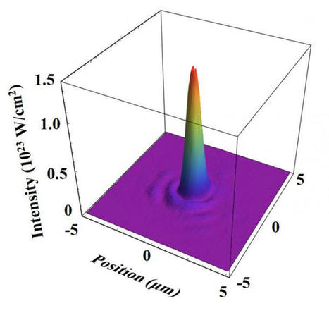
Scientists at the Institute for Basic Science have recently achieved the highest laser intensity in history. The record-breaking laser intensity over 10^23 W/cm^2 enable scientists to explore novel physical phenomena occurring under extreme physical conditions. Recently, laser scientists at the Center for Relativistic Laser Science (CoReLS) within the Institute for Basic Science (IBS) in South Korea realized the unprecedented laser intensity of 10^23 W/cm^2. This has been a milestone that has been pursued for almost two decades by many laser institutes around the world. An ultrahigh intensity laser is an important research tool in several fields of science, including those which explore novel physical phenomena occurring under extreme physical conditions. Since the demonstration of the10^22 W/cm^2 intensity laser by a team at the University of Michigan in 2004, the realization of laser intensity over10^23 W/cm^2 has been pursued for nearly 20 years. In general, achieving such a level of ultra-high laser intensity requires two things: laser with extremely high power output, and focusing that laser to the smallest spot as possible. While continuous-wave lasers are limited to megawatt-scale intensity, far higher peak power output (on the order of petawatt) is possible in pulsed laser systems by delivering the energy in the time scale as short as femtoseconds. In order to reach the goal of developing the world's most powerful laser, several ultrahigh power laser facilities with outputs of 10 PW and beyond, such as ELI (EU), Apollon (France), EP-OPAL (USA), and SEL (China), have been built or are being planned. A recent study from Osaka University even proposed a concept prototype for an exawatt class laser. Meanwhile, the CoReLS laser team has been operating a 4-PW laser system since 2016. This year in April 2021, they have finally achieved the record-breaking milestone of10^23 W/cm^2 by tightly focusing the multi-PW laser beam. Several special techniques have been employed to achieve this feat. The power intensity was maximized by using a focusing optics called an off-axis parabolic mirror, which was used to focus a 28 cm laser beam down to a spot only 1.1 micrometers wide. Such a diffraction-limited tight focusing can be obtained only with a clean laser beam without wavefront distortion. The CoReLS laser team, thus, made its PW laser beam as clean as possible using a set of deformable mirrors to correct the wavefront distortion of the PW laser. The CoReLS 4-PW laser is a femtosecond, ultrahigh power Ti:sapphire laser, based on the chirped pulse amplification (CPA) technique.
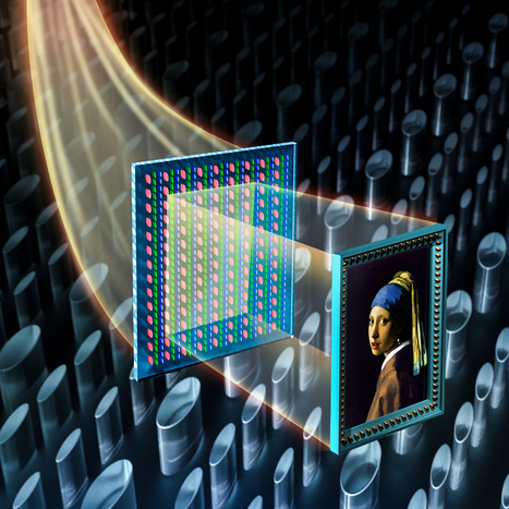
By shining white light on a glass slide stippled with millions of tiny titanium dioxide pillars, researchers at the National Institute of Standards and Technology (NIST) and their collaborators have reproduced with astonishing fidelity the luminous hues and subtle shadings of “Girl With a Pearl Earring,” Dutch artist Johannes Vermeer’s masterpiece. The approach has potential applications in improving optical communications and making currency harder to counterfeit. For example, by adding or dropping a particular color, or wavelength, of light traveling in an optical fiber, scientists can control the amount of information carried by the fiber. By altering the intensity, researchers can maintain t the brightness of the light signal as it travels long distances in the fiber. The approach might also be used to “paint” paper money with small but intricate color details that a counterfeiter would have great difficulty forging. Other scientists have previously used tiny pillars, or nanopillars, of varying sizes to trap and emit specific colors when illuminated with white light. The width of the nanopillars, which are about 600 nanometers in height, or less than one-hundredth the diameter of a human hair, determines the specific color of light that a pillar traps and emits. For a demanding test of such a technique, researchers examined how well the nanopillars reproduced the colors of a familiar painting, such as the Vermeer. Although several teams of researchers had successfully arranged millions of nanopillars whose sizes were tailored to transmit red, green or blue light to create a specific palette of output colors, the scientists had no way to control the intensity of those colors. The intensity, or brightness, of colors determines an image’s light and shadow — its chiaroscuro —and enhances the ability to convey impressions of perspective and depth, a signature feature of Vermeer’s work. Now, by fabricating nanopillars that not only trap and emit specific colors of light but also change its polarization by varying degrees, the NIST researchers and their collaborators from Nanjing University in China have for the first time demonstrated a way to control both color and intensity. The researchers, who include Amit Agrawal and Wenqi Zhu of NIST and the University of Maryland in College Park, and Henri Lezec of NIST, describe their findings in the September 20 issue of the journal Optica, posted online today.
This year marks the 20th anniversary of the first time an optical-frequency comb was used to measure the atomic hydrogen 1S-2S optical transition frequency, which was achieved at the Max-Planck-Institut für Quantenoptik (MPQ) in Garching, Germany. Menlo Systems, which was founded soon afterwards as a spin-off from MPQ, has been commercializing and pioneering the technology ever since. Today, optical frequency combs (OFCs) are routinely employed in applications as diverse as time and frequency metrology, spectroscopy, telecommunications, and fundamental physics. The German company’s fibre-based systems, and its proprietary “figure 9” laser mode-locking technology, have set the precedent for the most stable, reliable, robust, and compact optical frequency combs available on the market today. An optical frequency comb exploits laser light that comprises up to 106 equidistant, phase-stable frequencies to measure other unknown frequencies with exquisite precision, and with absolute traceability when compared against a radiofrequency standard. The most common and versatile approach to create an OFC is to stabilize an ultrafast mode-locked laser, in which pulses of light bounce back and forth in an optical cavity. The frequency spectrum of the resulting pulse train is a series of very sharp peaks that are evenly spaced in frequency, like the teeth of a comb. Through the so-called self-referencing technique, the first tooth of the comb – called the carrier-to-envelope offset frequency – is well fixed to a certain position. When the spacing of the comb teeth is referenced to a known frequency, such as the radiofrequency generated by a cesium atomic clock or a hydrogen maser, the absolute frequency of a light source can be accurately measured by interfering it with the nearest tooth on the comb with respect to the OFC reference. The device thus provides a way of making very accurate spectroscopic measurements of atomic and molecular transitions, and offers a versatile and unique way of comparing atomic clocks.
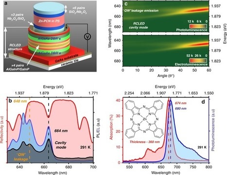
Polaritons are quasi-particles composed of a superposition of excitons and photons that can be created within a strongly coupled optical microcavity. Researchers now describe a structure in which a strongly coupled microcavity containing an organic semiconductor is coupled to a second microcavity containing a series of weakly coupled inorganic quantum wells. They were able to show that optical hybridization occurs between the optical modes of the two cavities, creating a delocalized polaritonic state. By electrically injecting electron–hole pairs into the inorganic quantum-well system, they were able to transfer energy between the cavities and populate organic-exciton polaritons. This approach represents a new strategy to create highly efficient devices for emerging ‘polaritonic’ technologies.
In 2015, researchers at the Harvard John A. Paulson School of Engineering and Applied Sciences (SEAS) developed the first on-chip metamaterial with a refractive index of zero, meaning that the phase of light could be stretched infinitely long. The metamaterial represented a new method to manipulate light and was an important step forward for integrated photonic circuits, which use light rather than electrons to perform a wide variety of functions. Now, SEAS researchers have pushed that technology further - developing a zero-index waveguide compatible with current silicon photonic technologies. In doing so, the team observed a physical phenomenon that is usually unobservable—a standing wave of light. The research is published in ACS Photonics. The Harvard Office of Technology Development has filed a patent application and is exploring commercialization opportunities. When a wavelength of light moves through a material, its crests and troughs get condensed or stretched, depending on the properties of the material. How much the crests of a light wave are condensed is expressed as a ratio called the refractive index—the higher the index, the more squished the wavelength. When the refractive index is reduced to zero the light no longer behaves as a moving wave, traveling through space in a series of crests and troughs, otherwise known as phases. Instead, the wave is stretched infinitely long, creating a constant phase. The phase oscillates only as a variable of time, not space. This is exciting for integrated photonics because most optical devices use interactions between two or more waves, which need to propagate in sync as they move through the circuit. If the wavelength is infinitely long, matching the phase of the wavelengths of light isn't an issue, since the optical fields are the same everywhere. But after the initial 2015 breakthrough, the research team ran into a catch-22. Because the team used prisms to test whether light on the chip was indeed infinitely stretched, all of the devices were built in the shape of a prism. But prisms aren't particularly useful shapes for integrated circuits. The team wanted to develop a device that could plug directly into existing photonic circuits and for that, the most useful shape is a straight wire or waveguide.
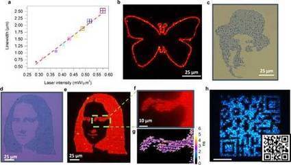
The use of quantum dots (QDs) in practical applications relies on the ability to precisely pattern QDs on substrates with desired optical properties. Typical direct-write printing techniques such as inkjet and gravure printing are limited in resolution (micron-scale), structural complexity, and require significant post-processing time.In new work, researchers at the University of Texas at Austin use laser-induced bubble printing to pattern CdSe/CdS QDs on plasmonic substrates with submicron resolution (<700nm line width), high throughput (∼10E4 µm/s) and strong QD-substrate adhesion.Not only is the bubble-mediated immobilization at the submicron scale stable, but the submicron-sized bubble's stability can be maintained over a large area. This technique is also compatible with flexible substrates and can be further integrated with smartphone to realize haptic integration. Finally, the emission characteristics of the QDs in terms of the emission wavelength and lifetime can be modified in real-time to achieve site-sensitive emission.The team, led by Yuebing Zheng, Assistant Professor of Mechanical Engineering and Materials Science & Engineering has been published in ACS Applied Materials & Interfaces ("High-Resolution Bubble Printing of Quantum Dots").
Light, when strongly concentrated, is enormously powerful. Now, a team of physicists led by Professor Jörg Schreiber from the Institute of Experimental Physics – Medical Physics, which is part of the Munich-Centre for Advanced Photonics (MAP), a Cluster of Excellence at LMU Munich, has used this energy source with explosive effect. The researchers focus high-power laser light onto beads of plastic just a few micrometers in size. The concentrated energy blows the nanoparticles apart, releasing radiation made up of positively charged atoms (protons). Such proton beams could be used in future for treating tumors, and in advanced imaging techniques. Their findings appear in the journal Physical Review E.
Surprising effect occurs when light is confined to fewer than three dimensions Photons can have half-integer values of angular momentum when they are confined to fewer than three dimensions. That is the conclusion of physicists in Ireland, who have revived an experiment first done in the 1830s to show that photons are not limited to having just integer values of angular momentum. The discovery could have applications in quantum computing and could also boost the capacity of optical-fibre data transmission. The angular momentum of light comes in two varieties: spin and orbital. Spin is associated with optical polarization, which is the orientation of light's electric-field oscillations. Orbital angular momentum rotates a light beam's wavefront around its propagation axis, giving it a corkscrew shape. Individually, the two types of angular momentum come in multiples of the reduced Planck's constant, ħ. For spin, those multiples are either +1 or –1, while the orbital variety can take any integer value. To date, physicists have assumed that a photon's total angular momentum is simply the sum of these two parts and that it therefore comes in integer multiples of ħ. But in the latest research, Paul Eastham of Trinity College Dublin and colleagues have shown that the total angular momentum can in fact take on half-integer values. Inspiration for the work, says Eastham, came from celebrations of the 200th anniversary of the birth of Irish mathematician William Hamiltonin 2005. Hamilton and physicist Humphrey Lloyd showed, in the 1830s, that a beam of light passing through a "biaxial" crystal takes on the shape of a hollow cylinder. The void at its centre is now known to be caused by the light acquiring orbital angular momentum. The bicentennial prompted renewed interest in this effect among physicists in Ireland, says Eastham, who joined Trinity College in 2009 and then started to think about exactly how such beams behave quantum-mechanically.
That the speed of light in free space c is constant has been a pillar of modern physics since the derivation of Maxwell and in Einstein’s postulate in special relativity. That the speed of light in free space c is constant has been a pillar of modern physics since the derivation of Maxwell and in Einstein’s postulate in special relativity. This has been a basic assumption in light’s various applications. However, a physical beam of light has a finite extent such that even in free space it is by nature dispersive. The field confinement changes its wavevector, hence, altering the light’s group velocity vg. Here, a group of scientists now reports the subluminal vg and consequently the dispersion in free space of Laguerre-Gauss (LG) beam, a beam known to carry orbital angular momentum. The vg of LG beam, calculated in the paraxial regime, is observed to be inversely proportional to the beam’s divergence θ0, the orbital order ℓ and the radial order p. LG beams of higher orders travel relatively slower than that of lower orders. As a consequence, LG beams of different orders separate in the temporal domain along propagation. This is an added effect to the dispersion due to field confinement. These results are useful for treating information embedded in LG beams from astronomical sources and/or data transmission in free space.
Fiber optics allow for the communication of data at the speed of light. But the amount of data that can be sent along any optic fiber is limited by how much information you can encode into the light wave travelling through it. Currently, optic fiber technology uses several different properties of light to encode information, including brightness, color, polarization and direction of propagation. But if we want to cram even more information through optic fiber, we need to use other features of light to encode more information, without disrupting the currently used properties. Such a feature could help boost the bandwidth of optic fiber technology, including our internet speed. If the light wave travelling through the optic fiber is twisted helically – like a spring – then it has an angular momentum, which is a measure of its momentum when it rotates around a point. But there was a major problem with using angular momentum to decode the information from the optic fiber in the past. We needed a material with tiny nanoscale helical structures that could detect the twisted light when present. A research team now published in Science, how the angular momentum of light at a nanoscale can be controlled by using an integrated photonic chip. So for the first time, we have a chip with a series of elaborate nano-apertures and nano-grooves that allow for the on-chip manipulation of twisted light. The helical design of these tiny apertures and grooves removes the need for any other bulky interference-based optics to detect the angular momentum signals. So if you send an optical data signal to a photonic chip, which is a microchip that uses light instead of electrons, then it is important to know where the data is going, otherwise information will be lost. Using this type of a nanophotonic chip, the researchers could precisely guide angular momentum data signals without losing the information they carry. What’s more, the angular momentum information of many different signals can be processed at the same time through the chip. This means we can potentially achieve an ultra-wide bandwidth, with six orders of magnitude of increased data access compared to current technology.
Researchers at the Institute of Quantum Optics and Quantum Information (IQOQI), the University of Vienna, and the Universitat Autonoma de Barcelona have achieved a new milestone in quantum physics: they were able to entangle three particles of light in a high-dimensional quantum property related to the "twist" of their wavefront structure. Just like Schrödinger's famous cat that is simultaneously dead and alive, all previous demonstrations of multi-particle entanglement have been with quantum objects in two discrete levels, or dimensions. The twisted photons used in the Vienna experiment have no such limit to their dimensionality, and can simultaneously exist in three or more quantum states. The three-photon entangled state created by the Vienna group breaks this previous record of dimensionality, and brings to light a new form of asymmetric entanglement that has not been observed before. The results from their experiment appear in the journal Nature Photonics.
Entanglement is a counterintuitive property of quantum physics that has long puzzled scientists and philosophers alike. Entangled quanta of light seem to exert an influence on each other, irrespective of how much distance is between them. Consider for example a metaphorical quantum ice dancer, who has the uncanny ability to pirouette both clockwise and counter-clockwise simultaneously. A pair of entangled ice-dancers whirling away from each other would then have perfectly correlated directions of rotation: If the first dancer twirls clockwise then so does her partner, even if skating in ice rinks on two different continents. "The entangled photons in our experiment can be illustrated by not two, but three such ice dancers, dancing a perfectly synchronized quantum mechanical ballet," explains Mehul Malik, the first author of the paper. "Their dance is also a bit more complex, with two of the dancers performing yet another correlated movement in addition to pirouetting. This type of asymmetric quantum entanglement has been predicted before on paper, but we are the first to actually create it in the lab."
The scientists created their three-photon entangled state by using yet another quantum mechanical trick: they combined two pairs of high-dimensionally entangled photons in such a manner that it became impossible to ascertain where a particular photon came from. Besides serving as a test bed for studying many fundamental concepts in quantum mechanics, multi-photon entangled states such as these have applications ranging from quantum computing to quantum encryption. Along these lines, the authors of this study have developed a new type of quantum cryptographic protocol using their state that allows different layers of information to be shared asymmetrically among multiple parties with unconditional security. "The experiment opens the door for a future quantum Internet with more than two partners and it allows them to communicate more than one bit per photon," says Anton Zeilinger. Many technical challenges remain before such a quantum communication protocol becomes a practical reality. However, given the rapid progress in quantum technologies today, it is only a matter of time before this type of entanglement finds a place in the quantum networks of the future.
Publication in "Nature Photonics": Multi-Photon Entanglement in High Dimensions: Mehul Malik, Manuel Erhard, Marcus Huber, Mario Krenn, Robert Fickler, Anton Zeilinger. Nature Photonics, 2016
http://dx.doi.org/10.1038/nphoton.2016.12.
A new method of building materials using light, developed by researchers at the University of Cambridge, could one day enable technologies that are often considered the realm of science fiction, such as invisibility cloaks and cloaking devices.
Although cloaked starships won't be a reality for quite some time, the technique which researchers have developed for constructing materials with building blocks a few billionths of a meter across can be used to control the way that light flies through them, and works on large chunks all at once. Details are published today (28 July, 2015) in the journal Nature Communications.
The key to any sort of 'invisibility' effect lies in the way light interacts with a material. When light hits a surface, it is either absorbed or reflected, which is what enables us to see objects. However, by engineering materials at the nanoscale, it is possible to produce 'metamaterials': materials which can control the way in which light interacts with them. Light reflected by a metamaterial is refracted in the 'wrong' way, potentially rendering objects invisible, or making them appear as something else.
Metamaterials have a wide range of potential applications, including sensing and improving military stealth technology. However, before cloaking devices can become reality on a larger scale, researchers must determine how to make the right materials at the nanoscale, and using light is now shown to be an enormous help in such nano-construction.
The technique developed by the Cambridge team involves using unfocused laser light as billions of needles, stitching gold nanoparticles together into long strings, directly in water for the first time. These strings can then be stacked into layers one on top of the other, similar to Lego bricks. The method makes it possible to produce materials in much higher quantities than can be made through current techniques.
In order to make the strings, the researchers first used barrel-shaped molecules called cucurbiturils (CBs). The CBs act like miniature spacers, enabling a very high degree of control over the spacing between the nanoparticles, locking them in place.
In order to connect them electrically, the researchers needed to build a bridge between the nanoparticles. Conventional welding techniques would not be effective, as they cause the particles to melt. "It's about finding a way to control that bridge between the nanoparticles," said Dr Ventsislav Valev of the University's Cavendish Laboratory, one of the authors of the paper. "Joining a few nanoparticles together is fine, but scaling that up is challenging."
The key to controlling the bridges lies in the cucurbiturils: the precise spacing between the nanoparticles allows much more control over the process. When the laser is focused on the strings of particles in their CB scaffolds, it produces plasmons: ripples of electrons at the surfaces of conducting metals. These skipping electrons concentrate the light energy on atoms at the surface and join them to form bridges between the nanoparticles. Using ultrafast lasers results in billions of these bridges forming in rapid succession, threading the nanoparticles into long strings, which can be monitored in real time.
"We have controlled the dimensions in a way that hasn't been possible before," said Dr Valev, who worked with researchers from the Department of Chemistry and the Department of Materials Science & Metallurgy on the project. "This level of control opens up a wide range of potential practical applications."
Via Anne Pascucci, MPA, CRA, Mark E. Deschaine, PhD, Jocelyn Stoller
|